On March 21, the Hefei Integrated Circuit Testing Industry Base officially started construction at the northeast corner of Xuetian Road and Ningxi Road in Hefei High-tech Zone.The project covers an area of about 41 mu, with a total construction area of about 50,000 square meters.It mainly builds production workshops, assembly workshops and related supporting service facilities. It is planned to be completed and delivered in May 2023.
Rendering of Hefei Integrated Circuit Testing Industry Base
Small chips are the core cornerstone of high-end manufacturing.Smartphones, computers, cars... all are inseparable from chips.
According to related reports, on the stage of chip R&D and manufacturing, Hefei is a "rising star", but it has a strong development momentum-the output value of the entire industry chain will be nearly 40 billion yuan in 2021, a year-on-year increase of about 30%.It has been listed as a national key development city for the integrated circuit industry by the National Development and Reform Commission and the Ministry of Industry and Information Technology.It has been approved as the country's first "Cross-Strait Integrated Circuit Industry Cooperation Pilot Zone" and the country's first batch of strategic emerging industry clusters for integrated circuits.
In recent years, Hefei High-tech Zone has accelerated the development of the integrated circuit industry and achieved remarkable results in order to realize the rapid development of the integrated circuit industry.At present, it has become the core bearing area for the development of the integrated circuit industry in Hefei.
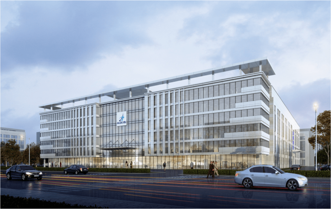
Hefei High-tech Zone Integrated Circuit Packaging and Testing Industrial Park
The integrated circuit packaging and testing industrial park constructed and operated by Hefei High-tech Co., Ltd.The total construction area is 78,000 square meters, and the total investment is 283 million yuan.Since the completion and delivery in December 2020, it has attracted many integrated circuit-related enterprises such as Hefei Ruihe Technology, Hefei Onst Technology, Century Jinguang, and Zijunguangheng to settle in and put into production.The contracted occupancy rate reached 100%, and the annual output value reached 500 million yuan;The integrated circuit headquarters base with a total construction area of 334,000 square meters and a total investment of 1.8 billion yuan is undergoing curtain wall construction. It is planned to be completed and put into use in December 2022.After completion, it will focus on introducing design and development, packaging and testing of integrated circuit chips and sensors, as well as upstream and downstream industrial chain-related enterprises in terminal applications such as smartphones and the Internet of Things, and strive to become an advanced integrated circuit industry base in China.
It is understood that after the Hefei Integrated Circuit Testing Industry Base project was completed and put into operation, it can form a test capacity of 90,000 pieces/month including integrated circuit 8-inch and 12-inch wafer testing, and a high-end integrated circuit chip test capacity of 100 million pieces/month for finished integrated circuit testing.It can provide 8-inch, 12-inch wafer testing and finished chip testing services of SOP, TSSOP, QFN, BGA, SIP and other specifications to meet the needs of high-volume IC R&D testing and mass production testing.Further promote the development of Hefei's integrated circuit industry chain in pre-package wafer testing and post-package finished product testing, and help create a "City of Chips".
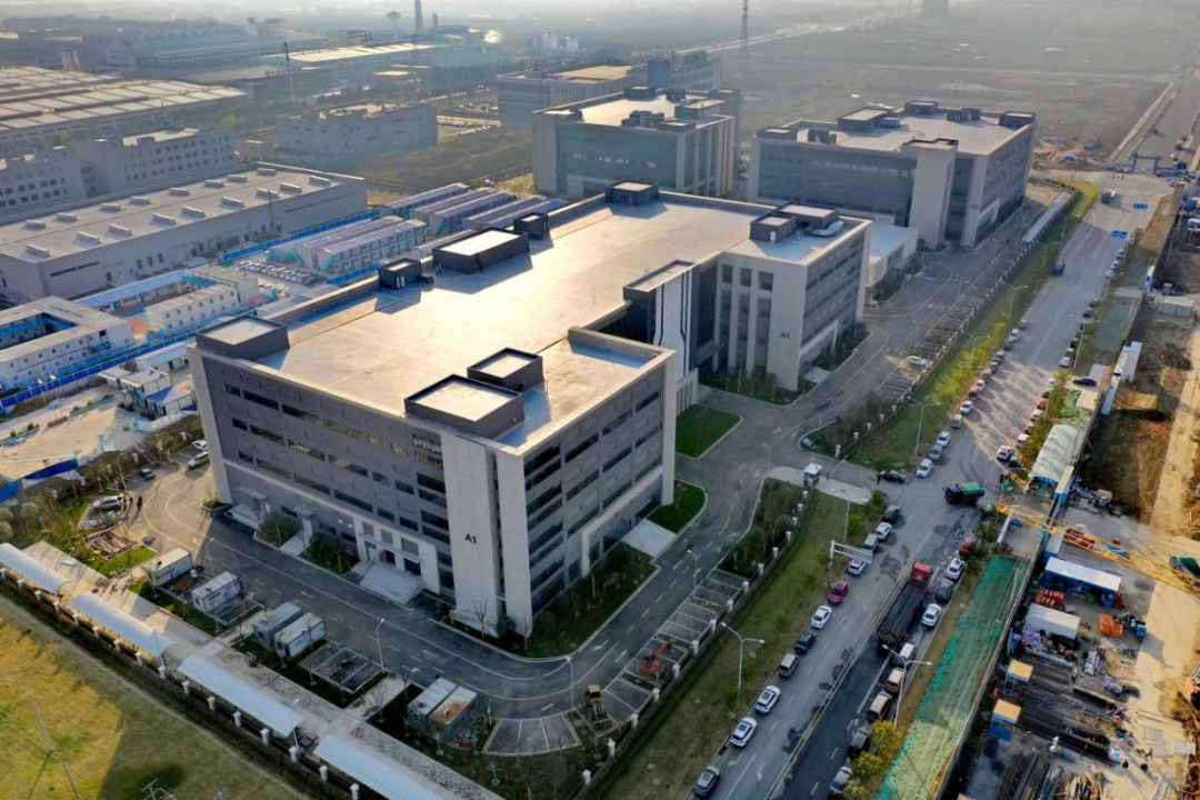
Hefei High-tech Zone Zhongan Chuanggu Phase II
Source of information and pictures: Hefei High-tech Release


 Park Dynamics